8+ Silicon Wafer Sds
Ad Find Over 15 Million Products at Grainger Today. An MSDS is a document that comes along with a hazardous chemical.
Material Safety Data Sheet Msds Defined
Ad Dynamic Process Group Specializes In The Precision Coring Resizing Of Wafers.

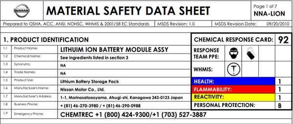
. Product Wafer MSDS Rev 22 06012022 Page 1 of 4 Revision date 06012022 MATERIAL. 647101 Silicon wafer single side polished N-type contains no dopant diam. Silicon Wafer Product Number.
Fast Delivery Next Day Shipping on Most Orders and Access to 247 Knowledgeable Support. Silicon wafers are Non-flammable. Safety Data Sheet SiliconSilicon Dioxide Wafer ACS Material LLC Version.
Our Products Services Are Designed To Satisfy All Our Customers. 14 rows Hyperpure silicon wafers are the basis for almost all semiconductor elements and. ACCIDENTAL RELEASE MEASURES 61.
Ad Up To 150mm Semiconductor Wafers 3-Step Polishing For High Quality. Product Name Silicon Reference Standard Solution 1000ppm Certified Cat No. All applicable American Elements product.
SU-8 is gently deposited on. PRODUCT AND COMPANY IDENTIFICATION Product name. Ad Up To 150mm Semiconductor Wafers 3-Step Polishing For High Quality.
WaferPro offers Prime Test Monitor SEMI standard and customized silicon wafers in all. Product Wafer MSDS Rev 30 06012022 Page 2 of 4 Revision date 06012022 MATERIAL. A vacuum line is used in order to firmly maintain the wafer in place.
Give Us A Call Today.

Rpzlcj2rts1rgm

Functional Supramolecular Systems Design And Applications Iopscience

Technology Development Resume Samples Velvet Jobs
Silicon Wafer Diameters Highly Doped And Lightly Doped
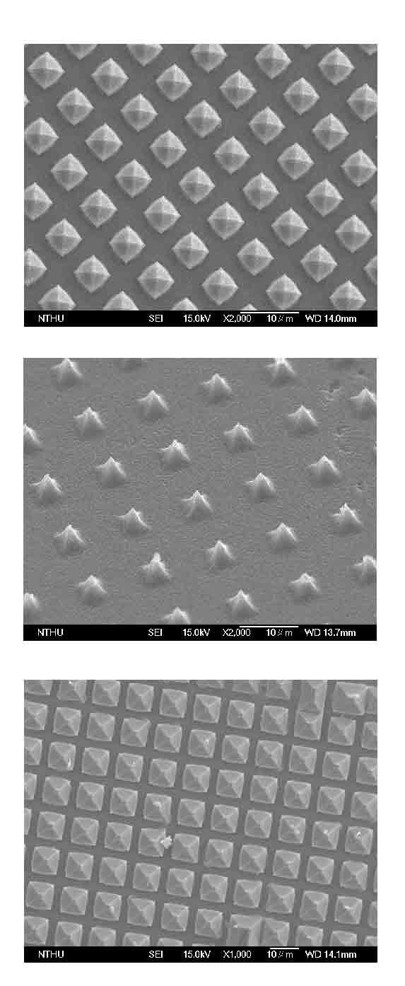
Patterned Silicon Wafers Universitywafer Inc

Silicon Wafers Preparation And Properties Sciencedirect

Silicon Wafer Single Side Polished N 100 No Dopant Diam 2in Thickness 0 5mm 7440 21 3

Palladium Nanoparticles In Polyols Synthesis Catalytic Couplings And Hydrogenations Chemical Reviews
What Scientific Research Are Silicon Wafers Used For

Tailoring Porous Silicon For Biomedical Applications From Drug Delivery To Cancer Immunotherapy Li 2018 Advanced Materials Wiley Online Library

Pdf On The Anomalous Peak In The Forward Bias Capacitance And Conduction Mechanism In The Au N 4h Sic Ms Schottky Diodes Sds In The Temperature Range Of 140 400 K Ahmet Kaya

Silicon Wafers Preparation And Properties Sciencedirect
Download Block Gsi Helmholtzzentrum Fur Schwerionenforschung

Silicon Wafer Posts Facebook

Silicon Wafer American Elements

Genesis And Tuning Of Ferromagnetism In Sno2 Semiconductor Nanostructures Comprehensive Review On Size Morphology Magnetic Properties And Dft Investigations Sciencedirect
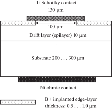
High Voltage 4h Sic Schottky Diodes With Field Plate Edge Termination Springerlink